
Published: October 31, 2022
Updated: March 28, 2025
As I described in “Volume 1: Semiconductor Miniaturization: What is Moore’s Law?,” the semiconductor industry first moved forward to realize Moore’s Law by seeking miniaturization. Since miniaturization means making semiconductor devices smaller, I cannot skip mentioning how semiconductor devices are made. So, I will briefly explain how to make semiconductor devices.
Table of Contents
Semiconductor Manufacturing Process
Lithography - Key Processes for Miniaturization -
Technology that Exceeds the Limits of Light Source Wavelengths - Immersion Lithography and Multi-patterning -
Overview of the Entire Two-dimensional Circuit Patterning Process
Etching: Another Key Process for Miniaturization
Supplementary Information
Volume 2: Semiconductor Miniaturization and Manufacturing Process
Semiconductor Manufacturing Process
Semiconductor devices are fabricated in the surface of a silicon (Si) wafer, which is a disk of single-crystal silicon with a thickness of about 0.5 mm to 1 mm. The manufacturing process for fabricating elements such as transistors and integrated circuits in the surface of a silicon wafer is generally referred to as a wafer process or simply a process in the industry.

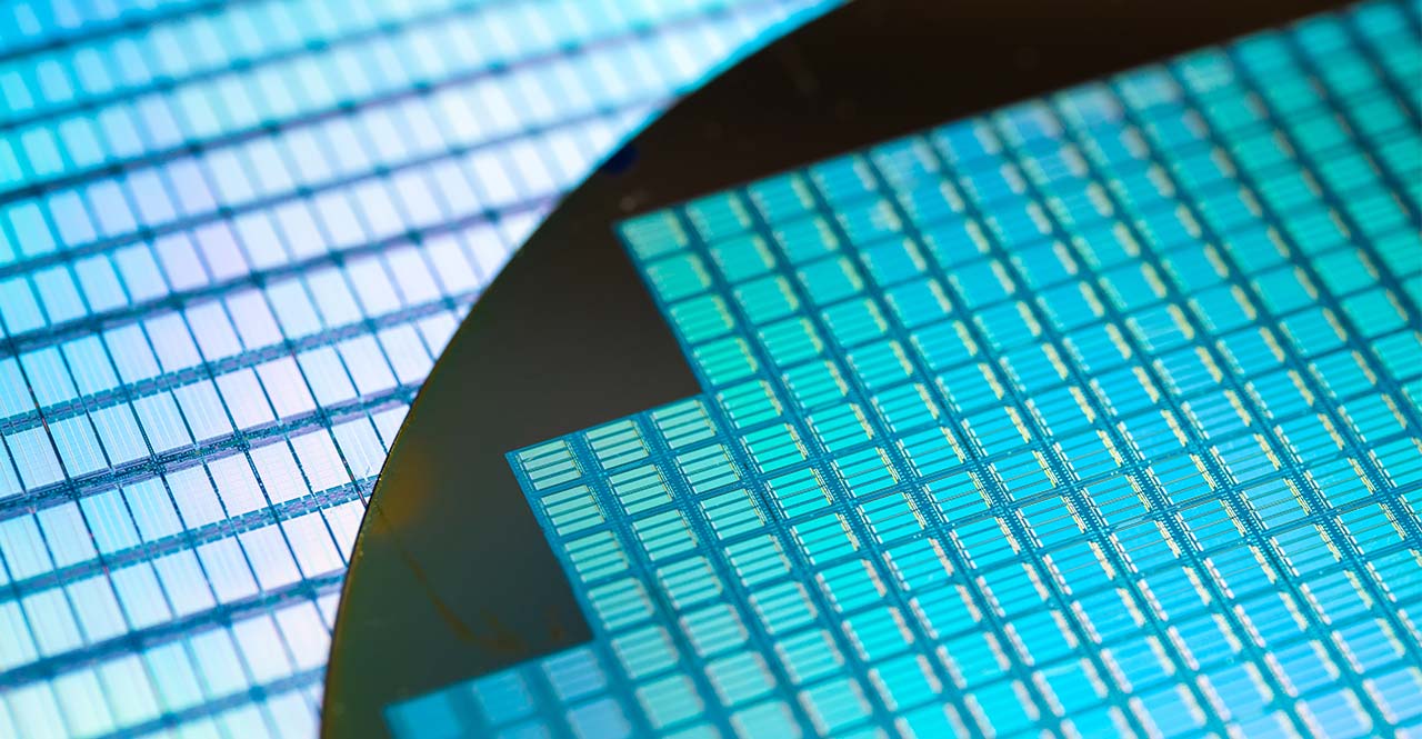
The surface of a silicon wafer is polished to a mirror finish and is normally stored in a cassette in a semiconductor fab and transferred between processes.
Since silicon itself does not have special properties such as amplification, a certain approach is required to fabricate elements such as transistors in the surface of a silicon wafer. This is impurity doping. One of the interesting properties of semiconductors is that their electrical properties can be changed by doping very small amounts of impurities. Additional impurities such as boron (B) or arsenic (As) to a silicon wafer creates regions which have opposite electrical properties called p-type and n-type. By combining them properly, elements such as transistors are fabricated.
Note: Silicon itself does not conduct much electricity, but it becomes more conductive when impurities are added. In contrast, metals become less conductive when impurities are added because the mechanism of electrical conduction differs between metals and semiconductors.
Note: A p-type and n-type semiconductor: A p-type semiconductor means positive, i.e., positive charges carry a current; an n-type semiconductor means negative, i.e., negative charges carry a current. A positive charge is called an electron hole (usually referred to simply as a hole), which is an empty spot left after an electron escaped, and a negative charge is an electron. For the two types of impurities mentioned above, the addition of boron (B) results in a p-type semiconductor, whereas the addition of arsenic (As) results in an n-type semiconductor.
In addition, to attach electrodes to a device for input and output of external electrical signals and to connect multiple elements to form an electronic circuit (i.e., an integrated circuit), it is necessary to fabricate metal interconnections, such as aluminum (Al) and copper (Cu), on the surface of a silicon wafer to flow electrical signals.
The figure below is a cross-sectional view of a certain semiconductor device. Semiconductor devices are generally made in region of a few µm to 10 µm above and below the surface of a silicon wafer.
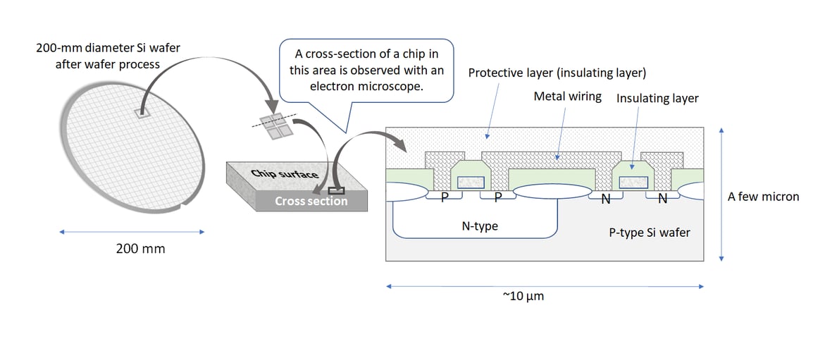
Note: This figure shows a device made with a very common process, not a state-of-the-art fine process, and is called CMOS technology, the most widely used device technology today. Also, although metal interconnections usually consist of two or more layers that cross each other (multilayer interconnections), one layer is shown for drawing convenience.
Processes to achieve what is described in this section can be categorized into three main types.
(1) Process to fabricate each element in a silicon wafer, such as impurity doping, heat treatment, oxidation, etc.
(2) Process to alternately deposit conductive layers such as metal to create interconnections that conduct electrical signals and insulating layers to insulate the interconnections.
(3) Process to manufacture two-dimensional circuit patterns of elements and interconnections.
By combining (1) and (3), each element that constitutes an integrated circuit is built in a silicon wafer, and by combining (2) and (3), integrated circuits are completed by connecting the elements with interconnections. The number of processes is estimated to be several hundred or more for the latest fine process.
A simple example of the process is shown below.
Process number from (1) to (3) in the figure corresponds to (1) to (3) described above.
First, a combination of (1) and (3) is used to fabricate an n-type region in a p-type silicon surface.
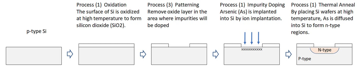
High temperature referred to here is generally approximately in the range of 1000°C.
Next, a combination of (2) and (3) is used to make an electrode connected to an n-type region.
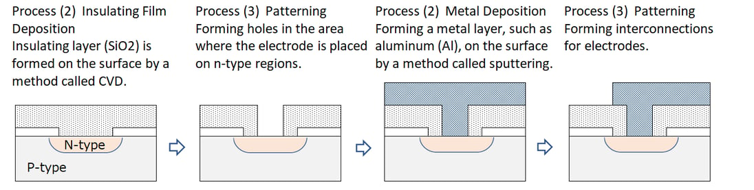
If an electrode is also connected to a p-type region, it becomes a diode.
Lithography - Key Processes for Miniaturization -
Miniaturization refers to the reduction of the size of the two-dimensional circuit pattern manufactured by the process (3) described above. The key process for manufacturing two-dimensional patterns is lithography. It is also called photolithography but is often referred to simply as lithography.
Note: Lithography: Originally the word means a technique to scribe characters or prints onto a flat stone.
In the lithography processes, the exposure is the key process to miniaturization. By using a precision optical instrument (exposure equipment), a circuit pattern formed on the surface of a square glass plate called a photomask is transferred to a photosensitive material (called resist) coated on a wafer. Although few people may know this, a negative film of old film cameras corresponds to a photomask, and photographic paper corresponds to a wafer. While in this case the image is magnified, it is reduced in the case of semiconductor exposure process. Resolution limit, which refers to the width of lines and the space between lines an exposure device can achieve, is mainly determined by the wavelength of the light source used in exposure equipment.
In the example of a simple process described above, three photomasks are used since the process (3) is performed three times. In the case of integrated circuits, more than 10 photomasks are usually used even for a simple process, and more than 30 photomasks are used for a slightly more complex process.
Note that simply exposing the material with an exposure equipment only causes some chemical changes in the areas of the photosensitive material that are exposed to light; no pattern has yet been formed. To form a circuit pattern on a photosensitive material, it is necessary to remove the light-exposed areas of the photosensitive material after exposure by a chemical process called developing.
A conceptual diagram of the exposure process is shown below.
Actual lenses are a combination of several lenses, not one.
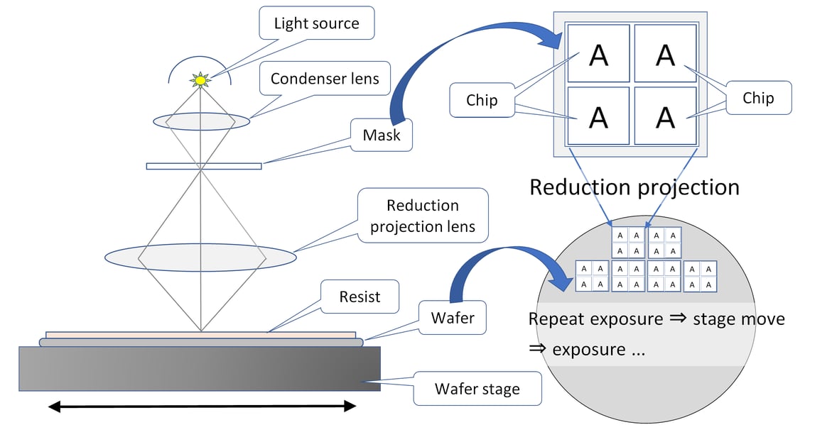
Note: The exposure method shown in this figure is called reduction projection lithography, which has become the mainstream since the 1980s. In the early stage (1960s), the exposure method was simple: a mask contacted with a wafer coated with a photosensitive material, and light was illuminated from above. In that case, the image size on a wafer was the same as that on a mask, not reduced, and it was called contact printing because a mask contacted with a wafer.
In the 1980s and 1990s, specific wavelengths emitted by mercury-arc lamp were the primary light source for exposure equipment. After using G-line (436 nm), I think I-line (365 nm) was used up to a minimum dimension of around 0.35 µm (350 nm). After that, 248 nm of a KrF excimer laser and 193 nm of an ArF excimer laser were used, and after a long development period, extreme-ultraviolet (EUV) 13.5 nm lithography finally came into mass production in late 2018 to 2019.
Note: In the optical system of EUV, optical lenses cannot be used, and reflective mirrors are used.
Technology that Exceeds the Limits of Light Source Wavelengths - Immersion Lithography and Multi-patterning -
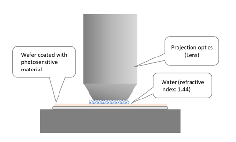
The 193 nm of an ArF excimer laser was used until the emergence of EUV in mass production, and the formation of fine patterns that were much smaller than the wavelength of the light source was required. It was achieved by immersion lithography and multi-patterning.
Immersion lithography is exactly as the word implies: the space between lens and a wafer is filled with a liquid medium. The wavelength of light in a liquid is the wavelength in air divided by the refractive index of the liquid. When water is used as the liquid, the refractive index of water is 1.44, so the wavelength of 193 nm is reduced by 0.69 times to 134 nm, thus forming a pattern with smaller dimensions. A schematic diagram of immersion lithography is shown below.
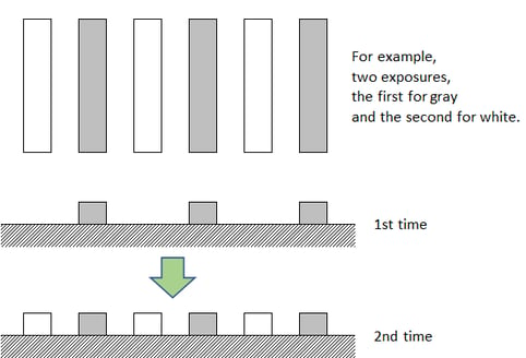
Multi-patterning is exactly as the word implies and is a technique of patterning in several steps. There are several methods for multi-patterning, but I will describe the simplest method here. For example, in the case of double patterning, a pattern can be exposed in two separate exposures as shown in the figure below, allowing a wider pattern spacing in each exposure and forming a high-density pattern that is not possible with a single exposure. However, because the number of times to divide the process will increase both the number of photomasks and the processes, so the cost will increase, and the lead time will be longer. It can be said to be a cutting-edge technology from the viewpoint that patterns below the resolution limit can be formed. However, it can also be said to be a painful measure from the viewpoint that it is necessary to repeat many times to achieve what has conventionally been done only once.
Overview of the Entire Two-dimensional Circuit Patterning Process
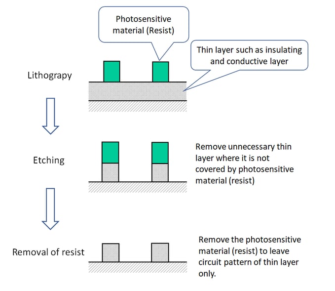
The lithography process described above is not a complete patterning process because it only forms a pattern on a photosensitive material. Accordingly, I will explain the entire two-dimensional circuit patterning process in a simple diagram here.
First, a pattern of photosensitive material is formed in the lithography process, followed by the removal of insulating film, conductive film, and other areas not covered by the photosensitive material in a process called etching. Finally, the photosensitive material is also removed to complete the formation of a two-dimensional circuit pattern.
Etching: Another Key Process for Miniaturization
Etching was performed in the early stages using chemical solutions such as acids (wet etching). However, this method cannot form fine patterns, so today, etching is mainly done using plasma generated by applying high voltage to gases or other methods (dry etching). For more details on plasma and dry etching, please refer to the supplementary information at the end of this article.
In the case of wet etching, as shown on the left side of the diagram below, the dimensions of circuit patterns such as insulating and conductive films formed by etching become narrower than those of the photosensitive material. This makes wet etching unsuitable for forming fine patterns. This occurs because etching progresses uniformly in all directions, such as vertical, horizontal, and diagonal, as indicated by the dashed arrows in the diagram.
To form fine patterns, etching must proceed straight down, precisely following the pattern of the photosensitive material, as shown on the right side of the diagram below. This is achieved using dry etching, which became widely adopted in the 1980s. No matter how much lithography technology advanced, without dry etching, fine patterns beyond approximately 3 µm to 2 µm could not have been realized.

I have briefly explained how semiconductor devices are made. In the next volume, I will explain how miniaturization has progressed.
Supplementary Information
Plasma and Dry Etching:
Plasma is a state of matter in which freely moving positively and negatively charged particles (such as electrons and ions) coexist while maintaining overall electrical neutrality. Atoms, which make up matter, consist of a nucleus and electrons orbiting around it. However, when the temperature becomes extremely high, these components separate, resulting in a state where electrons and positive ions move freely. This state is called plasma. Plasma is also referred to as the fourth state of matter, following solid, liquid, and gas.
The interiors of stars, such as the Sun, which make up the universe, are plasma, and it is said that more than 99% of the matter in the universe exists in plasma state. Natural plasma-related phenomena observed on Earth include auroras and lightning. In our daily lives, flames are plasma, and fluorescent lights emit light by utilizing artificially generated plasma.
As mentioned above, matter can turn into plasma when heated to high temperatures. Plasma can also be generated by applying a high voltage to induce electrical discharge. Electrical discharge refers to the process in which electrons and ions are generated in a gas by applying a high voltage, allowing a large current to flow. The plasma used in fluorescent lights and the plasma seen in lightning are formed through electrical discharge.
The plasma used in dry etching is also generated through electrical discharge by applying a high voltage. Broadly speaking, etching that does not use chemical solutions (liquids) is referred to as dry etching. However, in the semiconductor industry, dry etching is generally understood to mean plasma-based etching.
On March 28, 2025, the following updates were made:
1. In the section “Semiconductor Manufacturing Process,” an explanation was added regarding the behavior of semiconductors when impurities are introduced. Additionally, in the explanation of p-type and n-type semiconductors, it was noted that adding boron (B) results in a p-type semiconductor, while adding arsenic (As) results in an n-type semiconductor. A photo of silicon wafers stored in a cassette was also added.
2. A new section titled “Etching: Another Key Process for Miniaturization.” was added. Additionally, related supplementary information was added at the end of this article.
Click below to read this series.
Semiconductor Miniaturization:
Volume 1: Semiconductor Miniaturization: What is Moore’s Law?
Volume 2: Semiconductor Miniaturization and Manufacturing Process
Volume 3: Semiconductor Miniaturization and International Technology Roadmap
Volume 4: Semiconductor Miniaturization and Semiconductor Business
Volume 5: Semiconductor Miniaturization and Semiconductor Business (Part 2)
Volume 6: Semiconductor Miniaturization and Semiconductor Devices
Volume 7: Semiconductor Miniaturization: What is MOSFET Scaling?
Volume 8: Semiconductor Miniaturization: Limitations of MOSFET Scaling
Volume 9: Semiconductor Miniaturization and Analog Circuits
Shift to Larger Diameter Silicon Wafers:
Volume 10: Shift to Larger Diameter Silicon Wafers: How a Common Material, Silicon, Became a Main Player


Comment