
Published: May 23, 2025
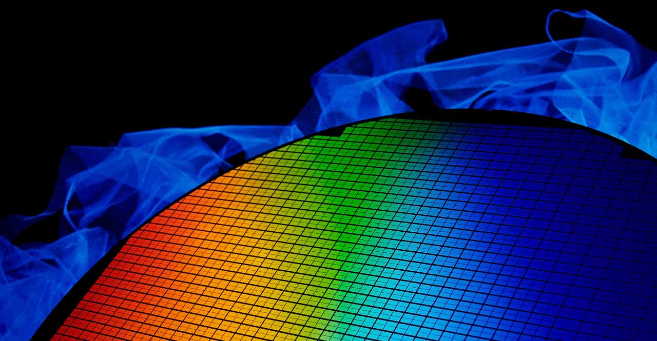
So far, I have discussed silicon (Si) itself and silicon wafers. In this final volume of the “Shift to Larger Diameter Silicon Wafers” series, I will talk about the main topic, the shift to larger diameter silicon wafers.
Table of Contents
Reasons for Larger Diameter
History of the Shift to Larger Diameter Wafers
Unrealized 450 mm Wafer
The Diameter of Silicon Wafers, in “inch” or “mm”
Why Are So Few Analog Products Using 300 mm Wafers?
Volume 12: Shift to Larger Diameter Silicon Wafers (Part 3): Reasons and History
Reasons for Larger Diameter
The primary reason for increasing wafer diameter can be summarized as “productivity improvement.” Increasing the wafer diameter increases the surface area of the wafer, which increases the number of chips per wafer. In addition, since the manufacturing cost per wafer does not increase significantly, the cost per chip is consequently reduced.
An example is shown in the figure below (upper part of the figure). In the example shown, the number of chips per wafer increases more than the wafer area ratio. This is because the chips protrude from the outer edge in the peripheral area of the wafer, as shown in the figure, resulting in a wasted area where chips cannot be placed. The smaller the wafer diameter, the greater the effect. An extreme example is shown in the lower part of the figure. Although this is an extreme example, it is a real possibility for specialized products. For large area chips, the benefits go beyond a simple increase in wafer area.


Wafer area ratio vs. chip count ratio
In Volume 1, I explained Moore’s Law, which states “the number of elements on a single chip will double in two years.” I also mentioned, “In order to realize Moore’s Law, increasing the chip area is one factor, but it is not enough. Therefore, it is necessary to increase the number of elements per unit area.”
In the “Semiconductor Miniaturization” series, I have discussed miniaturization as a method of increasing the number of elements per unit area. However, I have not talked about another approach: increasing the chip area.
If the wafer area remains the same while the chip area increases, the number of chips per wafer decreases. As a result, even if the same number of wafers are produced, the production volume of the product will decrease, and the cost per product will increase. However, by increasing the wafer diameter, if the wafer area and chip area increase at approximately the same rate, in other words, if the number of chips per wafer remains the same, then the same number of wafers can be used to produce the same number of products at the same cost.
An example of a microprocessor is shown below. The chip area has actually increased, so an increase in wafer diameter was probably essential for such products.
History of the Shift to Larger Diameter Wafers
Here is a look back at the history of the shift to larger diameter wafers.
I am not sure what the diameter of the world’s first silicon wafer was, but according to several sources, wafers around 20 mm in diameter were in use around 1960. This was right around the time that integrated circuits were invented.
The 1K-bit DRAM commercialized by Intel in 1970 used 2-inch wafers (approximately 50 mm in diameter). Since the chip area at that time was just under 10 mm2, simple calculations showed that a 2-inch wafer could yield about 200 chips. Starting in 1972, Intel switched to 3-inch wafers (approximately 75 mm in diameter).
When I joined the company in 1981, 4-inch (100 mm) wafers were used in our factory*. In the 1980s, the wafer size increased to 6 inches (150 mm) and in the 1990s to 8 inches (200 mm), but the company's shift to larger diameters stopped there. At the world's leading edge, 300 mm wafers were introduced around 2000, but further increases in wafer diameter did not progress, and the 300 mm era continues.
* Electronic Technology Development Center at Ricoh Osaka Plant, the predecessor of the former Ricoh Electronic Devices.
The following figure shows the trends of microprocessor chip area and wafer area. The vertical axis uses a logarithmic scale. The data for chip area is based on the Wikipedia English version of “Transistor count” page (https://en.wikipedia.org/wiki/Transistor_count). The figure shows that microprocessor chip area has increased year by year, and the wafer area has grown at a similar rate. The year of the points plotted for wafers in the figure is the approximate time of their introduction. The difference between the maximum chip area and the wafer area is about two orders of magnitude, which means that even for the largest area chip, about 100 chips can be obtained from a single wafer.

Microprocessor chip area trends
Unrealized 450 mm Wafer
In fact, 450 mm wafers were planned to follow 300 mm wafers. This was mentioned in the International Technology Roadmap for Semiconductors (ITRS), which I discussed in Volume 3, and was under active consideration. According to the initial roadmap, mass production should have been achieved in the 2010s. By around 2015, efforts were well underway toward mass production, and a consortium had been formed. I am unsure of the current situation, but it seems unlikely that they will be mass-produced in the near future.
To begin with, there are only a limited number of companies that manufacture products with large chip areas and high production volumes that would require the use of 450 mm wafers. It was also said that while the development of such manufacturing systems requires huge development costs, the number of customers who would use them is limited, and the development costs could not be recouped.
The Diameter of Silicon Wafers, in “inch” or “mm”
The diameter of a wafer is sometimes expressed in inches even today and sometimes in millimeters (mm). Since the semiconductor industry originated in the United States, where the yard-pound system is used, it is thought that inches were used initially. Even though it was changed to “mm” at some point, the use of inches has remained as a convention. In our company, we still use terms such as “6-inch” and “8-inch.”
For example, the diameter of a wafer called 8 inches is 200 mm, so it is not exactly 8 inches, but 200 mm divided by 25.4 mm equals 7.87 inches. It is not 8 inches, but an “approximately” 8-inch wafer.
Why Are So Few Analog Products Using 300 mm Wafers?
Although 300 mm wafers are considered the most advanced, not all products use 300 mm wafers. The products that primarily use 300 mm wafers are advanced digital products such as memory, processors, and FPGAs. In contrast, many factories that manufacture analog products still use previous generation wafers, such as 200 mm, 150 mm, or even smaller diameter wafers.
Although there have been some cases of 300 mm wafers being used for analog and discrete products recently, even today 200 mm, 150 mm and smaller wafers are often still used. While this is just my personal opinion, let me outline a few possible factors that could explain this.
(1) Unlike digital products, analog products tend to have longer lifetimes, so older processes with smaller wafer diameters continue to be used. This is especially true for products such as those for automotive applications, where change is difficult, and it is necessary to continue production under the same conditions. When I once asked a certain foundry in Taiwan why they still maintained a 6-inch factory, they gave a similar reason.
(2) Analog products generally do not require highly integrated, large-area chips as digital products do. For a single-function power management IC, the number of elements required is almost fixed and does not increase significantly, so the chip area does not increase in the same way as for processors. Therefore, I think the advantages of 300 mm are less for analog products than for digital products (of course, productivity is improving, so it does not mean there is no advantage).
(3) In the case of small chips such as power management ICs, the use of 300 mm wafers results in too many chips per wafer, and it would be difficult to manage production unless a large number of products with the same specifications were produced. In fact, when our company moved power management ICs to 8-inch wafers, there were some opinions that 8-inch wafers might not be necessary for power management ICs.
(4) Digital products often become uncompetitive if they are not converted to the latest processes, leaving factories with older processes idle. I think there are circumstances where such factories have been used to manufacture analog products. As I mentioned in Volume 9, miniaturization is not always beneficial for analog products, so even old processes for such digital products are often not a problem for analog products. I have heard that a foundry outside of Japan first set up its factories for digital products, and then gradually added processes for analog, high-voltage, RF, and other types of products to extend the life of the factories.
However, I believe that even analog products will gradually move to 300 mm wafers. During the semiconductor shortage that began in the fall of 2020 and continued for several years, it was said that there was a shortage of 200mm manufacturing capacity, and some products have probably started to move to 300mm. The processes used in the early 300 mm factories are no longer considered advanced processes, so even for non-digital products, those with relatively high integration and high volumes are likely to be (or may already be) manufactured on 300 mm wafers. While foundries that operate both 200 mm and 300 mm factories in particular are expected to drive the shift to 300 mm, analog products will continue to be manufactured on 200 mm factories because they are likely to be maintained for the foreseeable future.
This concludes the discussion of the second trend in semiconductors, “Shift to Larger Diameter Silicon Wafers.”
In the next volume, I will discuss the third trend, “horizontal specialization.”
Click below to read this series.
Semiconductor Miniaturization:
Volume 1: Semiconductor Miniaturization: What is Moore’s Law?
Volume 2: Semiconductor Miniaturization and Manufacturing Process
Volume 3: Semiconductor Miniaturization and International Technology Roadmap
Volume 4: Semiconductor Miniaturization and Semiconductor Business
Volume 5: Semiconductor Miniaturization and Semiconductor Business (Part 2)
Volume 6: Semiconductor Miniaturization and Semiconductor Devices
Volume 7: Semiconductor Miniaturization: What is MOSFET Scaling?
Volume 8: Semiconductor Miniaturization: Limitations of MOSFET Scaling
Volume 9: Semiconductor Miniaturization and Analog Circuits
Shift to Larger Diameter Silicon Wafers:
Volume 10: Shift to Larger Diameter Silicon Wafers: How a Common Material, Silicon, Became a Main Player
Volume 11: Shift to Larger Diameter Silicon Wafers (Part 2): How Silicon Wafers Are Made
Volume 12: Shift to Larger Diameter Silicon Wafers (Part 3): Reasons and History


Comment