
Published: June 28, 2022
Updated: March 10, 2025
Table of Contents
What Is a Semiconductor?
The Invention of Integrated Circuits and Moore's Law
Hello, my name is Yoshida of Nisshinbo Micro Devices Inc. and I will now write a blog.
I plan to write mainly about semiconductors and related topics in a way that even beginners can understand. I would like to start about major trends in the semiconductor industry.
Volume 1: Semiconductor Miniaturization: What is Moore's Law?
As for the major trends, I will focus on miniaturization, larger diameter wafers and horizontal specialization. I would like to explain miniaturization, with semiconductors, semiconductor processes, and semiconductor devices mentioned briefly.
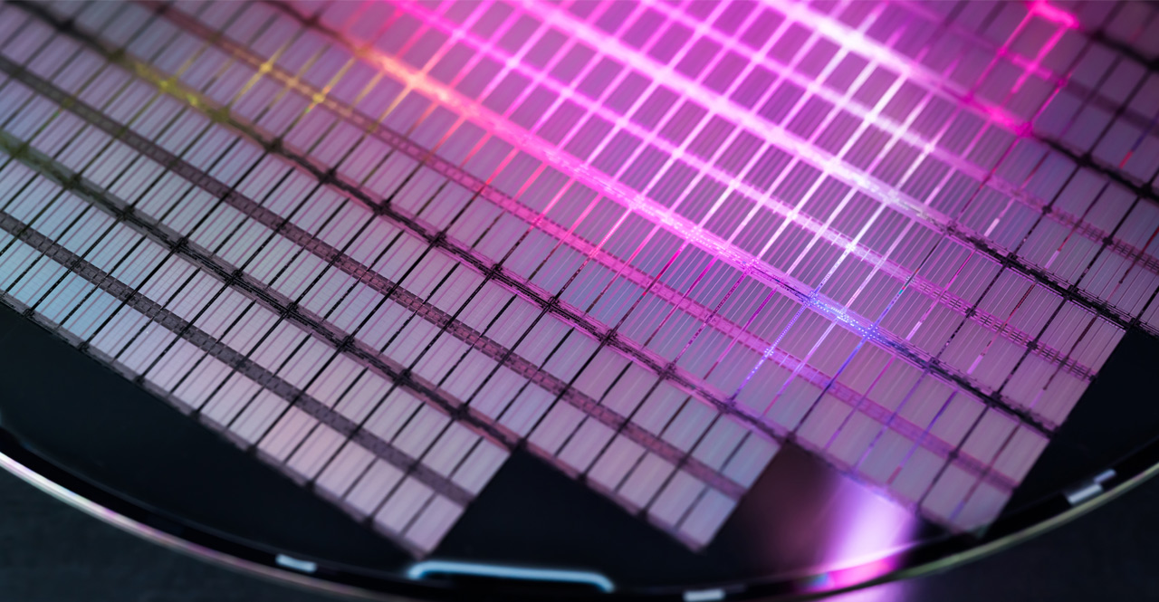
What Is a Semiconductor?
The term "semiconductor" originally referred to a material with properties between a conductor, such as metal, and an insulator, which does not conduct electricity, such as glass. The term "semiconductor" is also used conventionally to refer to "semiconductor devices" including single elements such as transistors and diodes using semiconductors, and including integrated circuits, which contain integrated these elements.
As semiconductor "materials", Ge (germanium) and Si (silicon) were both used in the early days, until around the 1950s. The transistor was invented at the end of 1947, and Ge was used at that time. In 1955, Tokyo Tsushin Kogyo (now Sony) commercialized the transistor radio, which also used Ge. However, subsequent research has established the superiority of silicon in terms of practical application. Nowadays, silicon is used almost universally for semiconductor devices, especially integrated circuits. The following topics are basically about semiconductor devices that use silicon.
However, for special applications, materials other than silicon (compound semiconductors) are used because their characteristics are superior to those of silicon in such applications. Radio frequency (RF) devices, or high-frequency devices, used in communications equipment and other applications have traditionally employed gallium arsenide (GaAs) or other materials that operate faster than silicon. In power semiconductors that handle high power, silicon was primarily used in the past, but materials with superior properties, such as silicon carbide (SiC) and gallium nitride (GaN), have begun to be adopted. SiC was adopted in inverters for Japanese railcars in the early 2010s, and its use in railways expanded after it was demonstrated to be highly effective in reducing equipment size and energy consumption. In 2020, SiC was adopted in the Shinkansen, Japanese bullet trains. Since the late 2010s, the adoption of SiC devices in electric vehicles (EVs) has increased, and SiC devices are now entering a phase of widespread use. On the other hand, GaN is used in compact, lightweight, and energy-efficient AC adapters and chargers for PCs and smartphones. As of the end of 2024, its primary application is in consumer products, but its use is expected to expand to power supplies for servers and on-board chargers (OBC) for electric vehicles (EVs).
Note: We offer GaAs products, please visit the following link for more details.
RF Device | Nisshinbo Micro Devices
Note: Also, please visit our columns on RF devices, linked below.

Connect Everything Wirelessly | Nisshinbo Micro Devices
The positions of the elements discussed in this section appear in the periodic table as shown below.

The Invention of Integrated Circuits and Moore's Law
At the end of the 1950s, the integrated circuit was invented, in which multiple elements are mounted on a single chip. The future of integrated circuits was indicated by a law called Moore’s Law. Moore's Law simply states that the number of elements on a single chip will double in two years. I think it is more appropriate to describe it as an "empirical rule" or "prediction" than a "law."
Note: "Doubling every two years" may not sound like much, but this is an exponential function, where the number increases "explosively" as the years go by.
This so-called Moore's Law was stated by Gordon Moore, one of the founders of Intel. He stated it in a 1965 article he contributed to the 35th anniversary issue of Electronics Magazine at the request of the magazine while he was at Fairchild Semiconductor, his former company. The request was a prediction of the semiconductor industry for the next ten years.
In studying the chips of the past, Moore noticed that the number of elements on the chip was "doubling every year," and predicted that this would continue and that the number would increase to 65,000 by a factor of 1,000 in 10 years. In 1975, ten years later, he predicted that by the end of the 1970s, the pace would drop to a "doubling every two years,", and this became Moore's Law, which continues to this day.
Note: Fairchild Semiconductor was founded in 1957 and Intel was founded in 1968. Moore was involved in the founding of both companies.
It was not called Moore's Law from the beginning, but it was later named by Carver Mead, a professor at California Institute of Technology. I do not think that Moore was aware of it at the time, but Moore's Law became a major guidepost for the direction that the semiconductor industry took. At some juncture, semiconductor companies began to compete fiercely to be the first to realize this law. Even if it was not clearly stated in the form of a law, this trend was probably inevitable so long as competition existed.
In order to realize Moore's Law, increasing the chip area is one factor, but it is not enough. Therefore, it is necessary to increase the number of elements per unit area. There are two main ways to achieve this: one is to reduce the size of the elements (in short, "miniaturization"), and the other is to build up the elements in three dimensions (in short, "three-dimensionality"). The semiconductor industry first pursued miniaturization to realize Moore's Law. However, in recent years, it has become increasingly difficult to maintain the trend of high integration through simple miniaturization alone, and three-dimensionality, including chip stacking, has become a reality.
To see how much of Moore's Law is actually being realized, I made a graph of the number of transistors on a chip of a typical product. The vertical axis is logarithmic, so the exponential function becomes a straight line on the graph. The data on transistor count is sourced from the English version of Wikipedia, "Transistor count" (https://en.wikipedia.org/wiki/Transistor_count).
If there are multiple products in the same year, the one with the highest number of transistors is plotted. Moore's Law states that the number of transistors doubles every year until 1980, and doubles every two years after 1980, which is shown by the blue line.
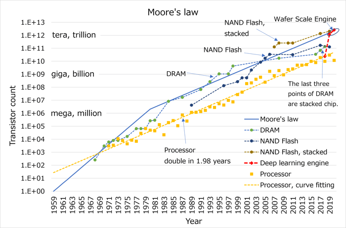
The graph shows that first, DRAM, then NAND flash memory (including chip stacks), have achieved a transistor count equal to or slightly higher than that predicted by Moore's Law. For processors, the trend continues to double in two years, although the number of transistors is below that predicted by Moore's Law.
Noteworthy is the "Wafer Scale Engine," a processor specialized for deep learning, in the upper right corner of the graph. It has almost the same number of transistors as Moore's Law predicts, except memory devices. How is a transistor count, about 100 times greater than that of a normal processor, achieved? The answer is to maximize the chip size. At present, we can only take one chip from the largest silicon wafer, which is 300 mm in diameter. The chip is a square inscribed in a 300 mm diameter circle, so it is impossible to make a larger chip than this product from a 300mm silicon wafer. This is an amazing product created by a US start-up company called Cerebras Systems.
 Because of its size over 20 cm square, it is a chip that no longer deserves the word "chip".
It is almost as large as a tablet.
Continue to the next article: Semiconductor Miniaturization and Semiconductor Process
Note: On March 10, 2025, in the section "What Is a Semiconductor?", the explanation of materials other than silicon (compound semiconductors) was added and revised.
Click below to read this series.
Semiconductor Miniaturization:
Volume 1: Semiconductor Miniaturization: What is Moore’s Law?
Volume 2: Semiconductor Miniaturization and Manufacturing Process
Volume 3: Semiconductor Miniaturization and International Technology Roadmap
Volume 4: Semiconductor Miniaturization and Semiconductor Business
Volume 5: Semiconductor Miniaturization and Semiconductor Business (Part 2)
Volume 6: Semiconductor Miniaturization and Semiconductor Devices
Volume 7: Semiconductor Miniaturization: What is MOSFET Scaling?
Volume 8: Semiconductor Miniaturization: Limitations of MOSFET Scaling
Volume 9: Semiconductor Miniaturization and Analog Circuits
Shift to Larger Diameter Silicon Wafers:
Volume 10: Shift to Larger Diameter Silicon Wafers: How a Common Material, Silicon, Became a Main Player


Comment