
Published: June 26, 2023
Updated: May 20, 2025
So far, I have used the words “semiconductor devices” to explain semiconductor miniaturization but have not explained them. In this volume, I would like to explain semiconductor devices in detail.
Table of Contents
Emergence of Transistors: From Vacuum Tubes to Solid-State Devices
What Is a Transistor?
Field-Effect Transistors and Bipolar Transistors
What Is a MOS Transistor?
What Is CMOS?
About Quantum Mechanics
Volume 6: Semiconductor Miniaturization and Semiconductor Devices
From Emergence of Transistors to CMOS, and Quantum Mechanics at the End
Emergence of Transistors: From Vacuum Tubes to Solid-State Devices
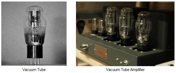
A transistor was invented at Bell Telephone Laboratories (hereafter Bell Laboratories) in the United States. Bell Laboratories was founded in 1925 as an affiliate of AT&T (American Telephone and Telegraph Company), a huge U.S. telecommunications monopoly. Its name was derived from Graham Bell, the inventor of the telephone. At that time, many devices called vacuum tubes were used in telephone systems. Since vacuum tubes were large and had high power consumption and short life span, they were expected to reach their limits sooner or later as the number of telephone lines increased.
Just at that time, rapid developments in solid-state physics based on quantum mechanics were revealing properties of semiconductors. Bell Laboratories pursued research with the specific goal of replacing the vacuum tube with a solid-state device using the semiconductor. Although temporarily interrupted by World War II, the transistor was invented on December 23, 1947.
Three inventors of the transistor were awarded the Nobel Prize in Physics in 1956. One of them, Dr. Bardeen, who later won the Nobel Prize in Physics for a theory of superconductivity, is the only person to have won the Nobel Prize in Physics twice as of 2024.
However, the transistor described here as invented is what is now called a bipolar transistor, not a MOS transistor used primarily in integrated circuits today.
At that time, Bell Laboratories was conducting research on field-effect solid-state amplification devices, which are today's field-effect transistors (FETs). MOS transistors are type of FETs. They didn't have sufficient knowledge of semiconductor surfaces and technologies to control them yet, so they repeatedly failed. In one of their experiments, they discovered an unintended current amplification phenomenon, which led to the invention of what is now known as bipolar transistors.
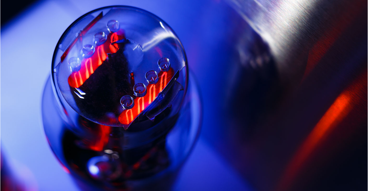
Note: Vacuum tube: A generic term for an electron tube with electrodes enclosed in a glass or metal container with a high degree of vacuum. Bipolar, triode, and multipolar tubes are available, and are used for wave detection, amplification, rectification, and oscillation. (English translation from Digital Daijisen published by Shogakukan) Typical height is a few cm to 10 cm.
What Is a Transistor?
Although I wrote about the invention of the transistor in late 1947, the word “transistor” did not exist at that time. The following year Bell Laboratories asked for a name for this new device and the name “transistor” was chosen, a combination of the words “transfer” and “resistor.”
What does a transistor do? In a single sentence, a transistor is “a device that can change (control) the current flowing through a transistor by changing the signal (voltage or current) that is applied to the input terminal.” With these features, transistors are used for amplifiers in analog circuits and as switches in digital circuits.
In order to understand transistors intuitively for a person without knowledge of physics, I will try to explain it as if it were water supply, an analogy that is often used. In the figure below, the water faucet (tap) is the device corresponding to a transistor. The water flow (electric current) can be controlled by twisting the knob of the faucet (corresponding to an input signal).
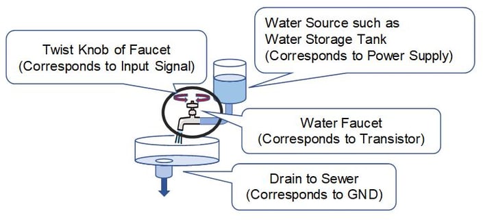
If the fully closed state is OFF and the fully open state is ON, it can be regarded as a switch. If you connect to a water source with large water pressure and use a large faucet with large water flow, you can greatly change the water flow (electric current) from the faucet just by slightly twisting the knob with your fingertip (slightly changing the input signal). If you replace this with electricity, you can use this in an amplifier.
Field-Effect Transistors and Bipolar Transistors
I mentioned that Bell Laboratories discovered an unexpected current amplification phenomenon while working on field-effect solid-state amplification devices (now field-effect transistors), which led to the invention of the device we now call bipolar transistors. The following figure illustrates both in a very simplified manner and in contrast to the water supply described in the previous section.
Note: Field-effect transistor: FET for short. More precisely, what we are describing here is an insulated gate field-effect transistor.

| The electric field created by applying a positive voltage to the gate electrode attracts electrons that slightly exist in the P-type region and collects them in the surface. This is called a channel. Through the channel, electrons flow from the right N-type region to the left N-type region. Since electrons have a negative charge, the current is the opposite, from left to right. |
Just applying a voltage between the entrance and the exit does not cause a current to flow, but applying a voltage to the input causes a large current to flow. At that time, a small current also flows from the input to the exit. The electrons carry the current, and they flow from the right N-type region to the left, opposite to the current. Most of the electrons flow to the entrance, but some flow to the input. |
According to this simplified diagram, the only apparent difference between the two is whether the input electrode is insulated or directly connected to the semiconductor. The bipolar transistor was invented during the research of field-effect transistors, so it is not surprising that they are similar.
In fact, when a MOS field-effect transistor integrated circuit is fabricated, a bipolar transistor is naturally formed as well. We call it a parasitic bipolar transistor. This is sometimes used in actual circuits. One example is a bandgap reference circuit that serves as a reference voltage source. Parasitic bipolar transistors can also be unintentionally activated and cause problems. One example of this is the latch-up phenomenon in CMOS, which can lead to damage in some cases.
What Is a MOS Transistor?
A field-effect transistor having a MOS structure at the gate electrode, to which input signal is applied, is called a MOS transistor. MOS is an acronym for Metal, Oxide, and Semiconductor. The structure is made by forming a thin “oxide” film on the surface of a silicon crystal (“semiconductor”) and placing a “metal” gate electrode on top of the oxide film.
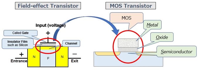
The gate electrode was metal initially, but later N- or P-type polycrystalline silicon came to be used. To be precise, it is strange to call it MOS because the gate electrode is not metal, but we call it MOS as well.
There are two types of MOS: P-channel type, in which a positive charge (holes) carries electricity; and N-channel type, in which a negative charge (electrons) carries electricity. They are often abbreviated as PMOS and NMOS, respectively.
It took more than 10 years after the invention of the transistor in 1947 for the MOS transistor to be put into practical use. The reason for this was the immaturity of silicon surface control technology, and the technology was first established and put to full-scale practical use in the 1960s. The first announcement was made by researchers of Bell Laboratories at a conference in 1960, and a patent was filed in the same year. Full-scale practical application of the technology seems to have been achieved in the mid-1960s. As I explained in vol. 4, MOS integrated circuits were first used in calculators in 1967, which means that they adopted a technology that had just been put into practical use.
The first IC used in calculators was a PMOS IC. Although NMOS was better suited for high-speed operation, it was difficult with the technology at that time, and therefore PMOS was used at first. Later, as the technology matured, NMOS became the mainstream. It was also in the 1970s that ion implantation equipment, which is now commonplace, was put to practical use.
Note: Ion Implantation System: As discussed in Volume 2, it is necessary to introduce impurities into semiconductors to manufacture semiconductor devices such as transistors. An ion implantation system is used for this purpose. As the name implies, this system ionizes impurity atoms, accelerates them with high voltage, and injects them into the target material. With an ion implantation system, the amount of impurities introduced can be precisely controlled.
What Is CMOS?
The term CMOS did not appear in the explanation of MOS so far, by the way. There is no transistor called a CMOS transistor. I remember a rookie engineer who once called it C-channel MOS. However, the C in CMOS is not for C-channel type but for complementary. As shown in the figure below (inverter circuit), a CMOS is a complementary combination of PMOS and NMOS to make a circuit.
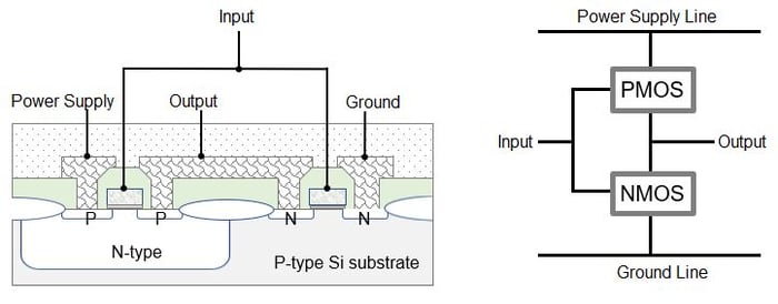
CMOS was presented at an international conference on solid-state circuits in 1963 and patented. However, because it is constructed by NMOS and PMOS, the wafer process is inevitably complex, and the circuit area is large. It took more than 10 years for CMOS to become widely used.
The major advantage of CMOS is its low power consumption, which is not explained here, so it was first used in electronic wristwatches and small calculators requiring low power consumption. CMOS LSIs were first used in calculators in 1972. It seems that CMOS was indispensable for battery operation. According to my memory (at least in our company, former Ricoh Electronic Devices), both NMOS and CMOS existed in the 1980s, but CMOS became the standard in the 1990s.
About Quantum Mechanics
Lastly, I would like to mention briefly about quantum mechanics.
The invention of the transistor would not have been possible without quantum mechanics, which was established between 1925 and 1926, and the development of semiconductor physics based on it. In other words, without quantum mechanics, there would be no PCs, smartphones, or the Internet, and today's digital society would not be possible. The United Nations has proclaimed 2025, the 100th anniversary of the birth of quantum mechanics, as the International Year of Quantum Science and Technology (IYQ 2025). We can see how quantum mechanics has had a huge impact on our world.
I believe that the scientists who established quantum mechanics were not thinking pragmatically but were doing research purely for the search for truth, which eventually led to a great social revolution. This is called fundamental research. Such a great achievement would not have been possible if research had been conducted with only short-term pragmatic considerations in mind. Our understanding of the fundamental laws governing the universe made this achievement come true.
Quantum mechanics along with the theory of relativity are the two major achievements (two major revolutions) of the 20th century in physics. Both theories were established at the beginning of the 20th century. The theory of relativity was the work of a single genius, Einstein, while quantum mechanics was established in the early 20th century by a number of physicists, especially young geniuses, and is a theory that describes the behavior of the very small unit of materials and energy (quantum) that form the universe, such as electrons and photons (quanta of light).
The names of physicists involved include Planck, Sommerfeld, Bohr, Born, Schrödinger, Pauli, Heisenberg, Dirac, and Fermi, and others. Pauli, Heisenberg, Dirac, and Fermi were in their mid-20s when quantum mechanics was established. All the scientists named here except Sommerfeld won the Nobel Prizes. Sommerfeld himself did not win the Nobel Prize, but four of his students, including Pauli and Heisenberg, did.
I cannot explain quantum mechanics in detail, but there are many interesting and mysterious things that common sense cannot imagine: An electron is a particle but also has the properties of a wave; Light is an electromagnetic wave but also has the properties of a particle (called a photon); The uncertainty principle states that the position and momentum of a particle cannot both be determined precisely. It is often said that the natural world is analog or continuous quantity, but in fact, according to quantum mechanics, energy, for example, has a minimum unit and is digital. However, the smallest unit is so small that it can be considered continuous.
In this volume, I briefly explained semiconductor devices, and lastly, I also briefly introduced quantum mechanics, without which there would have been no semiconductor device. In the next volume, I would like to talk about theoretical topics such as Dennard scaling law at the end of the talk about miniaturization of semiconductors.
On May 20, 2025, the following updates were made:
1. In the first section “Emergence of Transistors: From Vacuum Tubes to Solid-State Devices,” in the third paragraph, “Dr. Bardeen, who later won the Nobel Prize in Physics for a theory of superconductivity, is the only person to have won the Nobel Prize in Physics twice as of 2022.” is updated to “as of 2024.”
2. In the “What Is a MOS Transistor?” section, an explanation of ion implantation system is added after the last paragraph.
3. In the last section “About Quantum Mechanics,” it was added that the United Nations has proclaimed the year 2025, the 100th anniversary of the birth of quantum mechanics, as the International Year of Quantum Science and Technology (IYQ 2025).
Click below to read this series.
Semiconductor Miniaturization:
Volume 1: Semiconductor Miniaturization: What is Moore’s Law?
Volume 2: Semiconductor Miniaturization and Manufacturing Process
Volume 3: Semiconductor Miniaturization and International Technology Roadmap
Volume 4: Semiconductor Miniaturization and Semiconductor Business
Volume 5: Semiconductor Miniaturization and Semiconductor Business (Part 2)
Volume 6: Semiconductor Miniaturization and Semiconductor Devices
Volume 7: Semiconductor Miniaturization: What is MOSFET Scaling?
Volume 8: Semiconductor Miniaturization: Limitations of MOSFET Scaling
Volume 9: Semiconductor Miniaturization and Analog Circuits
Shift to Larger Diameter Silicon Wafers:
Volume 10: Shift to Larger Diameter Silicon Wafers: How a Common Material, Silicon, Became a Main Player
Volume 11: Shift to Larger Diameter Silicon Wafers (Part 2): How Silicon Wafers Are Made


Comment