
Published: February 14, 2024
Updated: June 5, 2025
As the last topic related to semiconductor miniaturization, I would like to talk about something a little more technical and theoretical. I will try to explain it as clearly as possible, so even if you have no technical knowledge, please spend some time with me.
Table of Contents
Dennard Scaling
What Happens If You Scale It by 1/2, for Example?
Why Do Digital Circuits Become Faster?
Supplementary Information
Volume 7: Semiconductor Miniaturization: What Is MOSFET Scaling?
Dennard Scaling
Moore’s Law, “the number of elements on a chip doubles every two years,” which we discussed in the first volume, was an empirical prediction. There is a theoretical law that underlies Moore’s Law. It is called “MOSFET scaling” and was published in a 1974 journal article by Robert H. Dennard of IBM. It is sometimes referred to as “Dennard scaling.”
I discussed the history of the semiconductor business and the evolution of semiconductor devices in volumes 4 through 6. The year 1974, when the MOSFET scaling was announced, was probably the time when MOS integrated circuit technology matured, the business began to take off, and miniaturization began in earnest.
Although miniaturization only makes transistors smaller and does not change the principle of operation at all, the MOSFET scaling theoretically showed that “smaller is better.” However, this is limited to digital circuits using MOS transistors.
Scaling means enlarging or shrinking a figure and so on, and there are scaling rules in other fields as well as semiconductors. For semiconductors, it is a guideline for scaling down a MOS transistor, and a theoretical explanation of how the characteristics of the MOS transistor and the performance of the circuit are affected when the transistor is scaled down according to the guideline.
If the size is reduced but the applied voltage is left unchanged, the device will not operate properly or will break down. Therefore, the applied voltage is also reduced at the same rate. This is the ideal result for digital circuits: The power consumption of the device is reduced while the integration of the device is increased. Therefore, for the same chip area, the power consumption does not increase, but the speed of the digital circuit is increased.
The following is a concrete explanation of the scaling rules. Please feel free to read on, even if you do not understand everything in detail, just to get a rough idea of what they mean.
What Happens If You Scale It by 1/2, for Example?
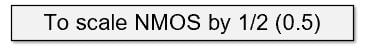
As an example, I will discuss scaling a MOS transistor by a factor of 1/2 (0.5).
1. Dimensions and Voltage Scaling

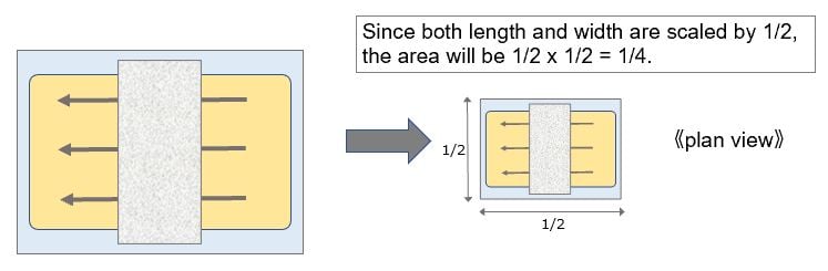
2. Area Scaling
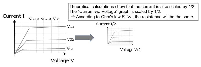
3. Current and Voltage Scaling
Note: While I will not go into detail because it would be too technical, the substrate impurity concentration (impurity concentration in the silicon wafer) is increased by a factor of 2. Impurity doping is briefly explained in the volume 2.
4. Power Consumption Scaling
According to 2 and 3, the following can be said about the power consumption.
- As shown in 3, both voltage and current are scaled by 1/2. Since the power consumption is the voltage multiplied by the current, the power consumption after scaling is 1/2 x 1/2 = 1/4, resulting in “one-quarter power consumption.”
- According to 2, since the area is also a quarter, it means that “the power consumption per unit area is the same even after scaling.” This means that if the area of the silicon chip is the same, the power consumption will remain the same even if the Si chip is highly integrated (see the figure below).
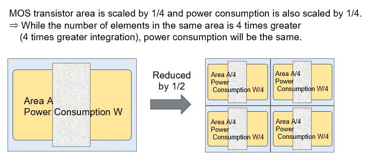
This is very important: Power consumption per unit area is the same even after scaling. If this is not true and power consumption increases, the amount of heat generated will increase and the temperature will rise, causing circuits to malfunction or fail. When this happens, miniaturization can be achieved, but high integration cannot. As a result, Moore’s Law no longer applies.
So far, we have seen that scaling down according to the MOSFET scaling allows high integration without increasing power consumption, and that Moore’s Law can be realized. Then, what about circuit performance?
The answer would be “digital circuits can achieve higher speeds.” It may seem that the signal takes less time to travel because the dimension of transistor is smaller, but it seems strange that it can be faster even though the current is reduced. Next, let me explain why it becomes faster.
Why Do Digital Circuits Become Faster?
As noted above, scaling also reduces the current, but the digital circuits become faster.
More speed with less current? Intuitively, some may wonder.
Indeed, if only the current is reduced while everything else remains the same, the circuit will obviously slow down. However, factors other than current that affect the speed of digital circuits are also scaled, and their effects are greater. Therefore, digital circuits become faster. To explain this in detail, it is necessary to consider how digital circuits transmit signals (information), which is explained below.
First, a brief description in technical terms is as follows.
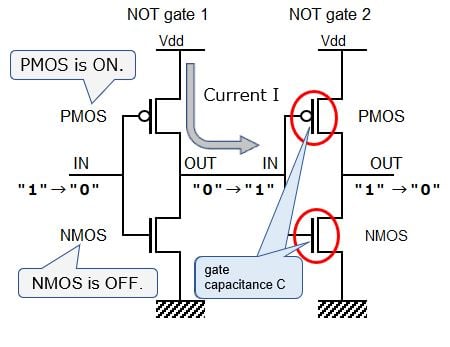
The speed of a digital circuit is determined by the charge/discharge time T of the gate capacitance C in the subsequent circuit. As a concrete example, consider the case where the output of a NOT gate (inverter), which is the simplest circuit, changes from “0” to “1”. See the figure below. When the input of the NOT gate 1 changes from “1” to “0,” the PMOS turns on and a current flows. This charges the gate capacitance C in the subsequent circuit, which causes the voltage to rise, and as a result, the output of NOT gate 1 (= input of NOT gate 2) changes from “0” to “1”.
Since Q equals CV from the formula for capacitance of the capacitor, the charging time T of the gate capacitance C when the output of the circuit changes from “0” to “1” is given by T = Q/I = CV/I, where V is the voltage corresponding to “1”, Q is the charge to be charged, and I is the charging current.
When scaled by 1/2, V and I are also scaled by 1/2. We can find out that the gate capacitance C is also scaled by 1/2 according to a simple calculation (see the additional explanation at the end of the text). Since each C, V and I is scaled by 1/2 in the charging time equation T = CV/I, we can find that T is also scaled by 1/2, which means the speed is doubled.
Note: For details, in addition to gate capacitance, parasitic capacitance such as wiring capacitance must also be considered.
To avoid getting too technical, the following is a roundabout explanation. They are in the following order: 1. What is a digital circuit, 2. How does a digital circuit work, and 3. Why does miniaturization make it faster?
1. What Is a Digital Circuit?
The antonym of digital is analog. Analog is a term for a continuous quantity, while digital is a term for a discrete quantity (a discontinuous value). For example, an analog clock displays time with a dial and hands, while a digital clock displays time with numbers, typically in minutes. It displays in one-minute increments, so 7:30 is followed by 7:31, for example.
 Analog clock (left) and digital clock (right)
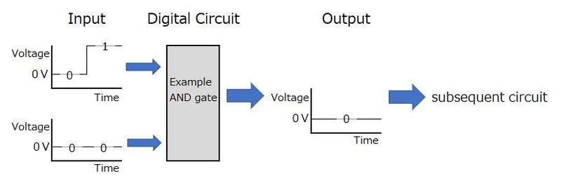
Digital circuits, by definition, are circuits that handle discrete values, and in most cases, they handle only two values, “0” and “1.” There may be one or more inputs, all of which are either “0” or “1.” Some processing is done on such inputs, and information consisting of “0” and “1” is output. Electrically, a low voltage and a high voltage represent “0” and “1” respectively. Specifically, a voltage close to zero V is considered “0” and a voltage close to the supply voltage is considered “1.” Digital circuits can express logic operations that deal with two states, true and false, and binary number operations.
Logic products are typical products that use digital circuits. Logic products range from small to large. Microprocessors (MPUs) and graphics processing units (GPUs) are typical state-of-the-art logic products.
In a logic product, the output of a simple basic digital logic circuit becomes the input of the subsequent circuit, and the output of that circuit becomes the input of the subsequent circuit. These are combined and repeated to perform complex processing.
The figure below shows an example of an AND gate with two input pins. The AND gate outputs “1” only when both inputs are “1.” Therefore, the output in the following example is “0.” An AND gate using CMOS technology can be configured with three PMOS and NMOS respectively.
2. How Does a Digital Circuit Work?
To create a high voltage equivalent to “1”, it is necessary to store electricity (positive charge). To turn “1” into “0”, it is necessary to release the stored electricity. The following is just an image, but to use water as an analogy, a bucket full of water is “1”, a bucket empty of water is “0”, and the depth of the water corresponds to the voltage.
Fast operation of a digital circuit means that it takes less time to store and release electricity. This is determined by the speed at which electricity is stored and released, or in other words, the speed at which electricity flows (current) and the amount of electricity to be stored.
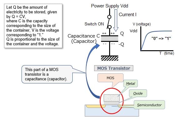
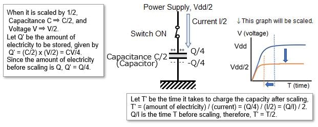
As those with a science background know, the amount of electricity Q is proportional to the size of a container storing the electricity C (capacity), and the required voltage V, which is given by Q = CV (see the text box in the figure below).
The figure below shows a schematic diagram for creating a high voltage equivalent to “1”. The part annotated “capacitance” is a container that stores electricity (capacitor in familiar terms). When the PMOS turns on and current flows from the power supply and stores electricity in the capacitance, “1” is output (= input to the subsequent digital circuit). For MOS digital circuits, the input terminal of the subsequent digital circuit is the gate electrode portion of the MOS transistor, which corresponds exactly to this capacitance.
3. Why Does Miniaturization Make It Faster?
The reason that miniaturization (scaling) makes it faster is that the current I in the figure above is smaller, and both the size of the container (capacitance) that stores the electricity and the voltage are also smaller, so the amount of electricity Q to be stored is much smaller.
Considering the scaling by 1/2 (see figure below), both the size of the container (capacitance C) and the voltage V are similarly halved, as shown in the additional explanation at the end of the text. In other words, the amount of electricity to be stored, Q = CV, is 1/2 x 1/2, which is 1/4. The time it takes to go from “0” to “1” is given by Q ÷ I, where Q is the amount of electricity, and I is the current. When scaled by 1/2, the amount of electricity and current are scaled by 1/4 and 1/2 respectively, so the time can be calculated as 1/4 ÷ 1/2 = 1/2, which means scaled by 1/2. In other words, it will be twice as fast.
I have discussed above that miniaturization (scaling) is a great advantage for digital circuits.
The advantages are summarized below.
1. High integration (reduced chip area for constant integration)
2. High speed
3. Low power consumption
Note: Please refer to the following section, “Supplementary Information,” for calculations of the power consumption of the digital circuits described here if you are interested.
Originally, this was going to be the last volume of the miniaturization series, but as I was writing it, the volume kept growing, so it will continue for two more volumes. In the next volume I will talk about how a good story like the MOSFET scaling does not last forever.
Supplementary Information
Calculation of Gate Capacitance C (Scaled by 1/2)
The gate capacitance is the capacitor in the red circle in the figure in “2. How does a Digital Circuit Work?” According to the capacitance formula, the gate capacitance is given by Cg = εA / Tox, where A is the electrode area, Tox is the thickness of the oxide in the figure, and ε is the permittivity of the oxide. Since A is an area, it is scaled by 1/2 x 1/2 = 1/4, and the thickness Tox is scaled by 1/2. After scaling, the capacitance is scaled by 1/4 ÷ 1/2 = 1/2. ε is not scaled because it is a material specific value.
Power Consumption and Scaling of Digital Circuits
As explained in the main text, digital circuits repeatedly store and release electricity. The output goes from 0 to 1 and back to 0, which means: electricity, or more precisely electric charge, flows from the power supply into a container or a capacitor (output changes from 0 to 1); and the stored electric charge is released to ground or GND (output changes from 1 to 0). Since the electricity or electric charge that flows from a power supply to ground during this one cycle is equal to the electricity stored in the container or capacitor, the average current is the electricity stored in the container or capacitor divided by the time of one cycle. Power consumption can be calculated by multiplying the average current by the voltage. The calculation is performed based on the assumption that charge and discharge occur continuously without a pause.
Let Q be the electric charge stored in the capacitor, so that Q = CV, and let T be the charge and discharge time. Then, the average current is given by I = Q/T = CV/T. Therefore, the power consumption is given by P = VI = V × (CV/T) = CV2/T.
When scaled to 1/2, as described in the main text, C, V, and T are reduced to 1/2 respectively, therefore the power consumption after scaling, P′, is given by:
P′ = (C/2) × (V/2)2/(T/2) = (1/4) × (CV2/T) = (1/4) × P.
This is the same 1/4 as described in the section “What Happens If You Scale It by 1/2, for Example?” The area is also reduced to 1/4, which means that the power per unit area is the same after scaling.
In general, the power consumption of a digital circuit is expressed as:
P ∝ CV2f,
where f is the operating frequency.
Let the period be T, so that f = 1/T. Therefore, the right-hand side of the expression becomes CV2/T, which is consistent with the previous result.
On June 5, 2025, the following updates were made:
1. Updated the content of the part “1. What Is a Digital Circuit?” in the section “Why Do Digital Circuits Become Faster?”
2. Added “Power Consumption and Scaling of Digital Circuits” to the section “Supplementary Information.”
Click below to read this series.
Semiconductor Miniaturization:
Volume 1: Semiconductor Miniaturization: What is Moore’s Law?
Volume 2: Semiconductor Miniaturization and Manufacturing Process
Volume 3: Semiconductor Miniaturization and International Technology Roadmap
Volume 4: Semiconductor Miniaturization and Semiconductor Business
Volume 5: Semiconductor Miniaturization and Semiconductor Business (Part 2)
Volume 6: Semiconductor Miniaturization and Semiconductor Devices
Volume 7: Semiconductor Miniaturization: What is MOSFET Scaling?
Volume 8: Semiconductor Miniaturization: Limitations of MOSFET Scaling
Volume 9: Semiconductor Miniaturization and Analog Circuits
Shift to Larger Diameter Silicon Wafers:
Volume 10: Shift to Larger Diameter Silicon Wafers: How a Common Material, Silicon, Became a Main Player
Volume 11: Shift to Larger Diameter Silicon Wafers (Part 2): How Silicon Wafers Are Made
Volume 12: Shift to Larger Diameter Silicon Wafers (Part 3): Reasons and History


Comment