
Published: February 14, 2024
Updated: June 23, 2025
In the previous volume, I talked about how miniaturization in accordance with MOSFET scaling brings great benefits to digital circuits. In this volume, however, I will talk about how a good story like this can never go on forever.
Table of Contents
Limitations of MOSFET Scaling
What Is Leakage Current?
Limitations of Supply Voltage Scaling
Limitations of Size Scaling: Gate Oxide Layer
To Overcome Limitations
Volume 8: Semiconductor Miniaturization: Limitations of MOSFET Scaling
Limitations of MOSFET Scaling
First, a recap of the last volume. The advantages of miniaturizing digital circuits according to MOSFET scaling are as follows.
1. High integration (reduced chip area for constant integration)
2. High speed
3. Low power consumption
However, a good story like that could never go on forever, which means that simple MOSFET scaling worked until about the year 2000, or about 0.18 µm (180 nm) in terms of process generation. (This can be interpreted differently by different people).
If we continue to miniaturize according to MOSFET scaling, the device size and supply voltage will continue to decrease toward zero. You can intuitively imagine that sooner or later a limit will be reached somewhere.
For example, as scaling proceeds and the size gets smaller and smaller, somewhere along the way it will fall below the interatomic distance or the size of the atoms, but in reality this is not possible.
Regarding two-dimensional patterns, before it gets smaller to that point, it becomes very difficult to form patterns by lithography, which I explained in Volume 2. I mentioned that EUV lithography technology has finally been put into practical use after a long period of development, but I have no knowledge at this point whether further technological advancement is prospected. I also mentioned in Volume 5 that EUV lithography equipment costs more than 10 billion yen, which I believe is beyond the economic limit for most companies, except for a few specialized ones.
The limits of size scaling and supply voltage scaling are explained in more detail below.
It is necessary to consider leakage currents to explain the supply voltage limits.
So, let's start with leakage current.
What Is Leakage Current?
In Volume 6, I mentioned that a MOS transistor is used as a switch in digital circuits. Ideally, a switch should have a current flow when it turns ON and no current flow (i.e., zero) when it turns OFF. Unfortunately, a MOS transistor has a small amount of current flow when it turns OFF. This is called leakage current.
Note: Since this current flows during the OFF condition, it is sometimes called off current or off leakage current.
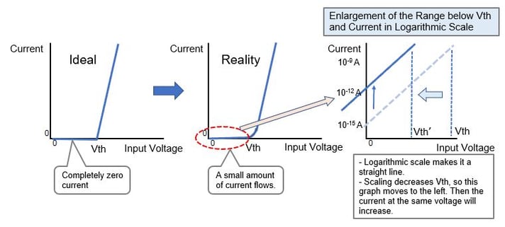
When the input voltage exceeds a certain voltage, the MOS transistor turns ON and a large current (ON current) flows. This input voltage at which the transistor turns ON is called a threshold voltage (Vth). When the input voltage is below the threshold voltage (Vth), the transistor is off, but leakage current flows as described above. The leakage current decreases exponentially and rapidly to zero as the input voltage is decreased toward 0 V, but it never completely reaches zero.
Note: Since the leakage current changes exponentially with the input voltage below the Vth, a graph of the current on a logarithmic scale will show a straight line (the rightmost graph in the figure below). Because it is the leakage current when the input voltage is below the threshold voltage, it is also called a subthreshold current or a subthreshold leakage current.
According to MOSFET scaling, the threshold voltage (Vth) will also be scaled to a smaller value. However, the behavior of the leakage current, i.e., the way of leakage current increase or decrease (exponential change) according to the variation of the input voltage below the threshold voltage (Vth), will not change much because it is roughly determined by a physical mechanism.
Therefore, when the threshold voltage (Vth) is decreased by scaling, the leakage current increases rapidly at the input voltage of 0 V, as shown in the rightmost graph in the figure below. The MOS transistor tries to reduce the current rapidly when the input voltage falls below the threshold voltage (Vth), but when the threshold voltage (Vth) is reduced by scaling and gets closer to 0 V, the current cannot be decreased completely even when the input voltage reaches 0 V.
As a result, you can see that the leakage current at the input voltage of 0 V was negligibly small in conventional MOS but will eventually become non-negligible as miniaturization (scaling) progresses.
Limitations of Supply Voltage Scaling
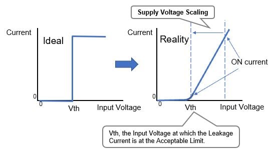
To briefly summarize what I discussed above, if miniaturization is carried out according to MOSFET scaling, the threshold voltage (Vth) also decreases. However, as the threshold voltage (Vth) decreases, the leakage current increases exponentially. If the scaling continues, somewhere the leakage current will reach a non-negligible level.
The only way to avoid this is to stop scaling the supply voltage at a certain level.
You may be thinking, “Why not just scale the supply voltage but not the threshold voltage (Vth), i.e., lower the supply voltage but not the threshold voltage (Vth)?”
In fact, it is possible. This suppresses the leakage current but does not increase the current when the transistor turns ON.
It would be good if the current would flow all at once at the instance of switching ON; that is, the moment the input voltage exceeds the threshold voltage (Vth). However, the current increases gradually with a certain slope. Here, the maximum input voltage is equal to the supply voltage. Therefore, as the difference between the threshold voltage (Vth) and the supply voltage becomes smaller, the input voltage will reach the supply voltage before the current has fully increased.
Even though the threshold voltage (Vth) is kept at a level where the leakage current is acceptable, it will eventually fall below the threshold voltage (Vth) if the supply voltage continues to be scaled. The limit will still be reached.
As far as I have experienced, the supply voltage for each process generation is scaled; 3.3V for a 0.35 µm (350 nm) process, 1.8 V for a 0.18 µm (180 nm) process, and 1.2 V for a 0.13 µm (130 nm) process. However, transistors of 90 nm and 65 nm processes use 1.2 V as the supply voltage, which does not decrease in accordance with scaling. If scaled; it should be about 0.65 V for a 65 nm. A leading-edge process in 2021 is 5 nm, but if it were scaled according to the process numbers, it would be about 0.05 V. This is a number that seems unlikely at any cost.
According to the International Roadmap for Devices and Systems (IRDSTM) 2023 Update, which I discussed in Volume 3, the supply voltage for logic devices is reported as 0.70 V in 2023 and remains at 0.60 V in 2037. Even if we can follow the roadmap, the supply voltage will not decrease much, and it is considered very difficult to reduce the voltage to even 0.60V. As I mentioned in the previous volume, I concluded that the power consumption per unit area is the same after scaling, based on the assumption that the supply voltage is scaled accordingly. If the supply voltage is not scaled, this conclusion does not hold, and power consumption (i.e., heat generation) becomes a very serious problem for advanced logic products.
Note: For the roadmap of the supply voltages mentioned above, see the Excel table on the “IRDSTM 2023: More Moore” page of the “International Roadmap for Devices and Systems (IRDSTM) 2023 Update.”
Limitations of Size Scaling: Gate Oxide Layer
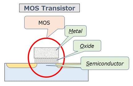
As discussed at the beginning, scaling of physical dimensions (size) also has its limits. The thickness of the gate oxide layer in MOS transistors (“Oxide” described in the figure below, oxide layer of Si) is also scaled and reached its limit first, partly because it was already thin before scaling.
In a 0.35-µm (350-nm) process, the thickness was already 10 nm or less, so if we simply scale it, the thickness will be impossibly thin, about 0.3 nm, the size of the interatomic distance or atoms in a 10-nm process. However, it is already too thin and loses its macroscopic “insulating film” property in the previous stage (around 45-nm process). This means that the film cannot be used as it is, because it cannot be insulated, and leakage currents will flow through it.
Even in terms of scaling physical dimensions (size), simple scaling breaks down.
To Overcome Limitations
In Volume 3, I wrote about a huge gap between the process name and the reality of leading-edge processes. Based on the story in this volume, we can say that although simple MOSFET scaling no longer applies; only the numbers in the process name are scaled.
Simple MOSFET scaling is no longer applicable, but new materials and technologies have been applied and transistors have been made three-dimensional to achieve higher performance. The ITRS, which I discussed in Volume 3, called this “Equivalent Scaling.”
In the example of the gate oxide film that I mentioned earlier, we used a new material with a high dielectric constant because, as a technical explanation, a material with a high dielectric constant (which we call a high-k material) can be used for a thicker film with electrically equivalent properties. In addition, it is becoming increasingly difficult to miniaturize MOS transistors with a planar (two-dimensional) structure as described so far. From the process generation of around 22 nm, transistors have a three-dimensional (3D) structure.
With the above, I have explained the limitations of MOSFET scaling in this volume. In the previous volume and this volume I explained the scaling of digital circuits, and in the next volume I would like to complete the series on miniaturization by discussing analog circuits and scaling.
On June 23, 2025,
Added a related topic at the end of the “Limitations of Supply Voltage Scaling” section.
Click below to read this series.
Semiconductor Miniaturization:
Volume 1: Semiconductor Miniaturization: What is Moore’s Law?
Volume 2: Semiconductor Miniaturization and Manufacturing Process
Volume 3: Semiconductor Miniaturization and International Technology Roadmap
Volume 4: Semiconductor Miniaturization and Semiconductor Business
Volume 5: Semiconductor Miniaturization and Semiconductor Business (Part 2)
Volume 6: Semiconductor Miniaturization and Semiconductor Devices
Volume 7: Semiconductor Miniaturization: What is MOSFET Scaling?
Volume 8: Semiconductor Miniaturization: Limitations of MOSFET Scaling
Volume 9: Semiconductor Miniaturization and Analog Circuits
Shift to Larger Diameter Silicon Wafers:
Volume 10: Shift to Larger Diameter Silicon Wafers: How a Common Material, Silicon, Became a Main Player
Volume 11: Shift to Larger Diameter Silicon Wafers (Part 2): How Silicon Wafers Are Made
Volume 12: Shift to Larger Diameter Silicon Wafers (Part 3): Reasons and History
Horizontal Specialization in the Semiconductor Industry
Volume 13: Horizontal Specialization in the Semiconductor Industry and the Rise of Fabless Companies


Comment