

Published: September 28, 2026
This article discusses chiplets, which were previewed at the end of my previous post, “Members of Advanced Logic Semiconductors.”
Table of Contents
What Is a Chiplet?
Products Using Chiplets
Examples of Chiplet Adoption Announcements
Why Chiplets?
Benefits of Chiplets: Flexibility
Enabling Chiplet Adoption: Standardization
Chiplet Integration Technology
Future Outlook
Volume 21: Miniaturization and Horizontal Specialization in the Semiconductor Industry (Special): What Is a Chiplet?
What Is a Chiplet?
Since around 2020, the term “chiplet” has come into widespread use in the field of advanced logic semiconductors. The processor manufacturer AMD is often credited with popularizing the concept.
Although the term “chiplet” does not have a strict definition, it is generally understood as follows:
“A design approach in which, instead of integrating all functions onto a single large semiconductor chip, those functions are divided among multiple smaller chips (chiplets), which are then interconnected (integrated) to operate as if they were a single chip.”
In short, it is one approach to enabling large and complex semiconductor devices. The term chiplet may refer either to individual small chips or to the architectural approach itself. More precisely, when referring to the approach, terms such as “chiplet architecture,” “chiplet approach,” or “chiplet technology” are more precise. By contrast, an approach in which all required functions are integrated onto a single chip, as well as products based on this approach, often described as a monolithic architecture, a monolithic integrated circuit (IC), or a monolithic system on a chip (SoC).
Note: There does not appear to be a universally accepted industry-wide definition, but the IEEE Electronics Packaging Society (EPS) has attempted to define chiplets (see link below).
https://eps.ieee.org/technology/definitions/
Note: The term “chiplet” does not have a universally agreed-upon definition in the industry, and its interpretation may vary. One common understanding is as follows:
General definition: A chiplet is an approach in which a traditionally monolithic semiconductor device is partitioned into multiple smaller chips, which are then combined to form a single system.
An SoC integrates functional blocks—circuits that implement individual functions—on a single chip. A chiplet, by contrast, combines separate chips that implement functional blocks within a package. Each functional block that makes up the product is implemented as an individual chip, and these chips are then combined to form the final product, so the approach can also be viewed as a modular approach. Functions A through E in the diagram below represent the functional blocks. The concept of chiplets is often likened to LEGO blocks, with each chiplet corresponding to an individual brick.
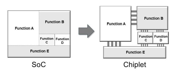
Conceptual diagram of a chiplet architecture
Regardless of whether it was used with the same meaning as today, the word itself has been used since before 2000 in the semiconductor industry. In fact, a search for academic papers containing the word reveals many papers from before 2000. For example, the term is used in a 1998 paper by IBM titled “Large Chip vs. MCM for a High-Performance System,” published in IEEE Micro. The usage in that paper appears to be similar to its present-day meaning.
There has been long debate over whether to integrate all functions into a single chip or implement them using multiple chips. Terms such as MCM (Multi-Chip Module), which also used in the IBM paper mentioned above, and SiP (System in Package), discussed in the final section (“What Is an SoC?”) of the previous post, have been used for many years. These terms refer to approaches for implementing functions or systems using multiple chips. In this sense, the ideas underlying chiplets are not particularly new.
Incidentally, the English word chiplet is formed by adding the suffix -let, which denotes something small to the word chip. For example, a booklet is a small book, and a piglet is a baby pig. An applet is a small program that runs within a host application, and chiplet can be thought of in a similar way.

Piglet (example of the suffix -let meaning “small”)
Products Using Chiplets
As discussed in the previous section, the term chiplet has been used in the semiconductor industry since before 2000. It came into widespread use around 2020, largely after AMD adopted the chiplet approach in its processors.
In 2021, AMD presented a paper titled “Pioneering Chiplet Technology and Design for the AMD EPYC™ and Ryzen™ Processor Families” at the ACM/IEEE 48th Annual International Symposium on Computer Architecture (ISCA).
In the title, “EPYC” and “Ryzen” are AMD processor brands. According to the paper, EPYC was the first product to which AMD applied a chiplet-based design approach. Since then, Intel has also adopted this approach to some of its products. However, as far as I am aware, it has not been used in smartphone SoCs from companies such as Qualcomm or MediaTek. Although the term has attracted considerable attention, chiplet adoption remains limited to the most advanced logic devices from only a small number of manufacturers as of early 2025.
Examples of Chiplet Adoption Announcements
In the previous section, it was noted that products adopting chiplet were still limited as of early 2025. However, several announcements of chiplet adoption have been reported between 2023 and 2024. The following examples are listed from newest to oldest. Three of the four examples are automotive products.
1. In November 2024, Renesas announced the first product in its fifth-generation R-Car series. Renesas stated that the R-Car is an automotive SoC featuring neural processing unit (NPU) and a graphics processing unit (GPU), which are powerful AI accelerators. The company also stated that additional chiplets to this configuration can further enhance AI processing performance. Mass production is scheduled for 2027.
2. The Advanced SoC Research for Automotive (ASRA) was established in Japan in December 2023 to conduct research and development on automotive SoCs using chiplet technology. Fourteen Japanese companies are participating, including six automotive manufacturers, three automotive electronics suppliers, and five semiconductor-related companies. The goal is to develop chiplet technology by 2028 and deploy SoCs in mass-produced vehicles by 2030.
3. Socionext is a Japanese fabless semiconductor company that provides custom SoC solutions. In October 2023, Socionext announced plans to collaborate with Arm and TSMC to develop CPU chiplets for use in custom SoCs for various markets. The plan was to start providing engineering samples (ES) in the first half of 2025.
4. In May 2023, NVIDIA and MediaTek announced a collaboration on developing automotive SoCs. MediaTek stated that it will integrate GPU chiplets from NVIDIA into its SoCs and supply them to automakers and other customers.
Note: Strictly speaking, when using chiplets, it is not a true system-on-chip. However, the term SoC is often still used. Since the chiplets are integrated to operate as if they were a single chip, it could therefore be regarded as a single chip, so the term SoC would still be used. Alternatively, in my personal view, it might be reasonable to consider it an abbreviation for “System on Chiplets.”

Use of chiplet technology in automotive SoCs is being explored.
Why Chiplets?
Although not discussed in detail so far, yield (the proportion of functional chips) is extremely important in the semiconductor industry. Unfortunately, not every chip on a wafer is functional, and defective chips cannot be repaired. Poor yield limits production volume and increases costs, which negatively affects business performance. Conversely, improved yield increases production volume and lowers costs. Therefore, improving yield is one of the most critical tasks for engineers in semiconductor fabs.
As illustrated in the simple example below, yield is strongly dependent on chip area: the larger the chip area, the lower the yield. As mentioned in Volume 12, the chip area of microprocessors has been increasing. While I may not be fully up to date with the latest developments, yield is likely a significant concern, particularly for cutting-edge processors with large chip areas fabricated using highly complex, leading-edge processes.
For example, if the area marked with an ‘X’ in the figure below contains a defect, such as a broken circuit pattern or a short circuit, the chip containing the defect is a defective chip. In the case of the wafer on the right, there are 20 chips, of which 8 are defective and 12 are functional. Therefore, the yield (the percentage of functional chips) is 12 ÷ 20, which is 60%. Even if defects occur at the same locations as on the right wafer, the chip area is one quarter, meaning the yield is 90%. Consequently, a larger chip area leads to a lower yield, whereas a smaller chip area leads to a higher yield. A good fab and manufacturing process have fewer defects, or ‘X’s, as shown in the figure below. Activities aimed at reducing this number of defects are known as yield improvement activities.
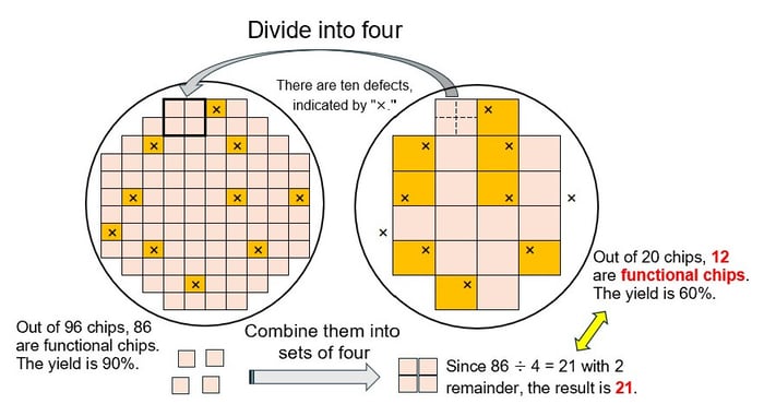
Yield improvement using chiplet architecture
The cost per wafer for leading-edge processes is extremely high, making poor yield a major issue. One approach to addressing this is the use of chiplets. Consider the figure above, where the right side represents a large processor or SoC, and the left side shows the same device divided into four chiplets (for simplicity, each is assumed to have the same function). In the case of the large processor on the right, only 12 functional chips can be obtained. However, when divided into four chiplets, 21 functional chips can be produced. This represents an increase in output of 1.75 times. Since cost is inversely proportional to the number of functional chips, cost decreases to approximately 57%. This represents a substantial improvement. This was likely a major factor behind AMD’s adoption of chiplets.
Additionally, partitioning a design into chiplets provides manufacturing benefits beyond improving yield. When all functions are integrated into a single chip, even blocks that do not require leading-edge processes must be fabricated using costly leading-edge processes. By using chiplets, however, functional blocks that do not require the most advanced processes can be manufactured using more cost-effective processes. These can then be combined with chiplets fabricated using leading-edge processes, reducing overall cost. Furthermore, chiplets manufactured by different companies can be combined.
However, the discussion above applies to cases where chip area is large and yield is poor. When chip area is small and yield is good, such considerations are not necessary. Without going into detail, there are additional costs associated with partitioning into chiplets. Therefore, using chiplets when yield is already good would likely increase costs. As noted earlier in the section on “Products Utilizing Chiplets,” chiplets are not used in smartphone SoCs from companies such as Qualcomm and MediaTek, to the best of my knowledge. This is likely because their chip areas are significantly smaller than those of PC and server processors.
Benefits of Chiplets: Flexibility
As mentioned above, using chiplets can significantly reduce the cost of processors and SoCs with large chip areas fabricated using leading-edge processes. Chiplets also offer additional benefits.
The most significant benefit is likely flexibility in product development. This can be illustrated with a familiar example.
Example 1, Cars:
A car’s functionality can be enhanced by adding manufacturer or dealer options, while a lower-cost configuration can be achieved by choosing the standard model without options. This kind of flexibility is also possible in semiconductor devices by using chiplets.
Example 2: Udon and soba (Japanese noodles)
By changing the toppings, you can create a variety of dishes, such as tempura soba (soba topped with tempura) or kitsune udon (udon noodles topped with seasoned fried tofu). Similarly, chiplets enable similar flexibility in semiconductor devices.
The examples presented in the section, “Examples of Chiplet Adoption Announcements,” appear to leverage these benefits. In Example 1, the Renesas approach (the R-Car automotive SoC) is analogous to adding a manufacturer option to a car: additional chiplets can be added to achieve higher performance.
Similarly, in Example 4, MediaTek’s plan to integrate NVIDIA GPU chiplets into its automotive SoC reflects the same concept, where components from other manufacturers can also be incorporated.
In Example 3, Socionext’s CPU chiplets, developed with Arm and TSMC, are analogous to plain udon or soba. Customers can add “toppings” (chiplets) to create customized “udon” or “soba” (custom SoCs) tailored to their needs. In Example 2, the ASRA consortium aims to develop the technologies and frameworks needed to enable automotive SoCs with the kind of flexibility illustrated in Examples 1 and 2.

Soba or udon (main chiplets) combined with various toppings (optional chiplets) to meet diverse customer requirements (left); examples of soba with topping combinations (right)
Enabling Chiplet Adoption: Standardization
To enable industry-wide adoption of chiplet technology rather than limiting its use to individual companies, connection methods between chiplets must be standardized. In other words, standardization is essential.

Standardized connection methods enable diverse products through chiplet combinations
One of the most well-known standardization initiatives is the Universal Chiplet Interconnect Express (UCIe). According to the UCIe website (Home | UCIe Consortium), UCIe is “an open specification that defines the interconnect between chiplets within a package.” In March 2022, the following ten industry-leading companies announced the establishment of a consortium to advance this specification and foster an open chiplet ecosystem. At the same time, the approval and availability of the UCIe 1.0 specification were announced.
Advanced Semiconductor Engineering, Inc. (ASE), AMD, Arm, Google Cloud, Intel Corporation, Meta, Microsoft Corporation, Qualcomm Incorporated, Samsung, and Taiwan Semiconductor Manufacturing Company (from the UCIe press release titled “Leaders in semiconductors, packaging, IP suppliers, foundries, and cloud service providers join forces to standardize chiplet ecosystem”)
As of early 2025, the board consists of the original 10 companies, along with Alibaba and NVIDIA, bringing the total to 12 members. In addition, there are two other membership tiers: Contributor Members and Adopter Members. These tiers include more than 100 companies. Renesas, ASRA, Socionext, and MediaTek, which are mentioned in the section “Examples of Chiplet Adoption Announcements” are members of one of these two groups. Furthermore, Renesas’s R-Car chiplets and Socionext’s chiplets are designed to be connected via UCIe. Several automobile manufacturers are also among the members. As of March 11, 2025, UCIe 2.0 has been released.
Chiplet Integration Technology
To integrate chiplets and treat them as a single chip, multiple chiplets must be interconnected, requiring interconnections between them.
As illustrated in the figure below, advanced logic products such as processors are mounted on package substrates. The substrate already contains wiring that connects the chip terminals to the package terminals. Therefore, one approach is to route inter-chiplet interconnects through the substrate without requiring new technologies. Another approach is to use a small chip dedicated to inter-chiplet connections (a bridge), or a separate chip that serves as both a mounting base and interconnect layer (an interposer). This approach requires fabricating a bridge or interposer in addition to the functional chiplets, increasing cost, particularly for interposers. However, this approach enables finer interconnects than those achievable in package substrates. The most suitable method is selected based on each manufacturer’s design philosophy, product requirements, and the characteristics of the available approaches. These technologies are used not only for chiplets but also for integrating conventional monolithic chips.
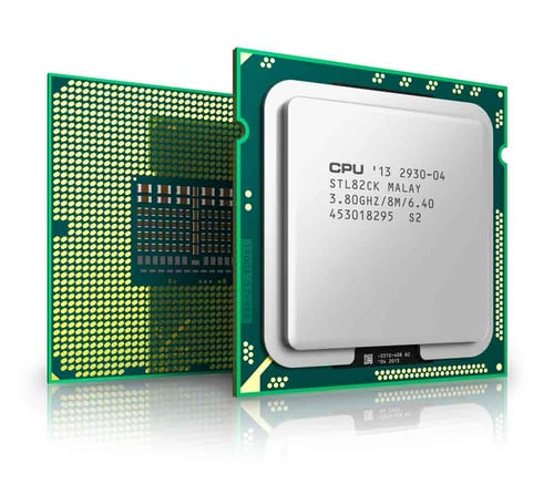
Processor illustration (left: rear view, right: front view)
- Over 1,000 gold-colored terminals arranged in a regular pattern on the back of the green substrate
- Multiple wiring layers within the green substrate connecting chip terminals to the backside terminals
The above points are summarized in the table below. In addition to the methods listed here, various other approaches that do not use package substrate wiring have been proposed. Examples include interposers made from different materials and combinations of interposers and bridges. Chip stacking techniques are also sometimes employed.
| Inter-Chiplet or Inter-Chip Wiring Technologies | ||
| Using Package Substrate Wiring | Using Dedicated Interconnect Chips | |
| Using an Interposer | Using a Bridge | |
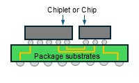 |
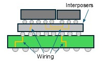 |
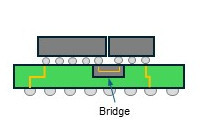 |
| 1 | 2 | 3 |
Note: Chiplets and chips are mounted in a face-down configuration and connected to the substrate or interposer.
Note: This is a conceptual diagram; dimensions and structural details are not to scale.
Inter-chiplet wiring technologies
The following examples show devices that integrate chiplets or chips using Types 1 through 3 in the table above. The figures illustrate the arrangement of chiplets or chips on the package substrate. These are schematic diagrams, and sizes and other details are not to scale.
Example of Type 1 in the Table Above: Using Package Substrate Wiring
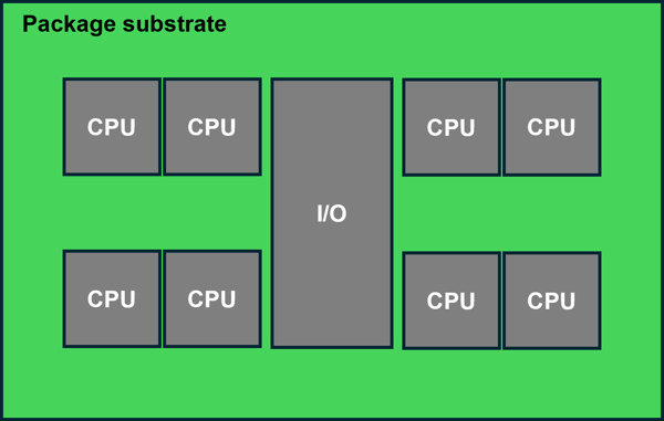
AMD 2nd Generation EPYC Processors
The processor is divided into eight CPU chiplets and one I/O chiplet. Splitting the CPU into smaller chiplets helps prevent cost increases due to lower yield. CPU chiplets are manufactured using the state-of-the-art 7nm process at the time, while the I/O chiplet uses a 12nm process, as it does not require the most advanced node. Additionally, product variants are created by adjusting the number of CPU chiplets. This approach leverages the advantages of chiplets mentioned earlier. As a result of various constraints and product requirements, this design uses package substrate wiring.
Example of Type 2 in the Table Above: Using an Interposer
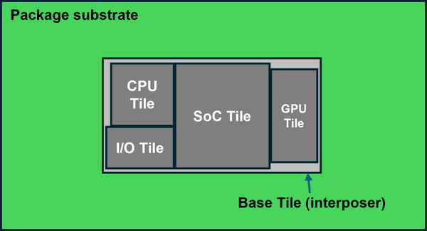
Intel Core Ultra processors
A separate chip, known as an interposer, is used to interconnect the chiplets. A separate chip, known as an interposer, is used to interconnect the chiplets. If treated as a single chip, it can be regarded as a conventional chip mounted on a package substrate. Intel refers to each chiplet as a “tile,” and these tiles are arranged adjacent to one another. Tiles are manufactured by both TSMC and Intel using different process technologies. This approach leverages the advantages of chiplets mentioned earlier.
Example of Type 3 Shown in the Table Above: Using a Bridge
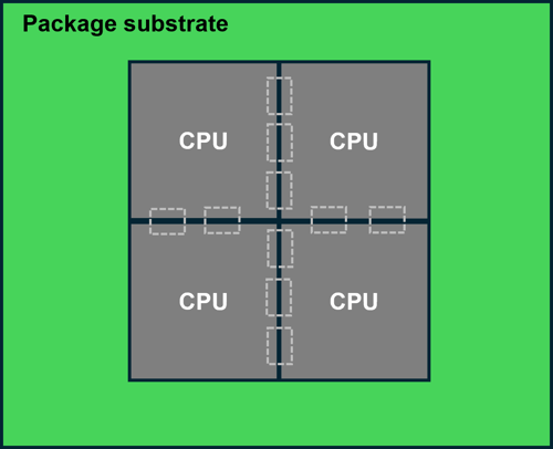
Intel 4th generation Xeon processors
The dashed square regions (ten in total) at the connection points between the four CPU chips in the figure above represent bridges. As shown in the cross-sectional diagram in the table above, these bridges are embedded in the package substrate beneath the chips. In this case, each CPU chip is relatively large and may not strictly be considered a chiplet. However, Intel refers to them as “tiles,” similar to the previous example. Compared to the chiplet-based approach described earlier, this configuration offers limited manufacturing or product development advantages typically associated with chiplets. Based on available information, the number of CPU chips appears to be fixed, and there are no variants created by changing this number. Rather than dividing a large chip into smaller chiplets, this approach can be better understood as combining large chips to form a larger system. Although this interpretation may not be definitive, some sources also suggest that it is not strictly appropriate to classify this as a chiplet-based design, while others do treat it as such.
It is widely recognized that the approach of relying solely on miniaturization and increasing chip area is reaching its limits in cutting-edge processors. As a result, more products are emerging that integrate multiple chips or chiplets into a single package.
NVIDIA’s GPU products integrate GPUs and DRAM within a single package using the Type 2 approach described above. Furthermore, Blackwell, which entered volume production in the second half of 2024, connects two large chips to operate as a single chip. Although this GPU integrates multiple chips, it is not based on a chiplet approach and is therefore not typically considered a chiplet. That said, because Blackwell consists of two chips forming a single GPU, it is sometimes regarded as a chiplet. However, Blackwell does not appear to target the manufacturing or design advantages discussed here. Instead, it appears to focus on improving processing performance by combining two chips.
Note: As mentioned earlier, the term “chiplet” is not clearly defined. As a result, some products are widely recognized as chiplets, while others are subject to differing interpretations. Additionally, the technologies for integrating chiplets discussed in this section are often referred to as chiplet technology.
Future Outlook
In the future, or ideally, a vision has emerged in which a wide variety of chiplets are available and can be combined like building blocks to create system LSIs. However, significant challenges remain, and it will take time. While the industry appears to be moving in this direction, it remains unclear whether this vision will ultimately become a reality.
Closing Remarks
Normally, this is where I would introduce the next post. However, this will be the final post. There are two reasons. First, it marks a natural conclusion after covering the major trends in the semiconductor industry, such as miniaturization, larger wafer sizes, and horizontal specialization. Second, I will soon be concluding my nearly 45-year career*. In the first post, I wrote, “I would like to start about major trends in the semiconductor industry.” I expected this discussion to wrap up in two or three posts at most, but it has grown to 21. I never imagined it would take so many posts, so even I am surprised. I started writing in 2020** and have spent more than a thousand hours researching and writing over the past five years. Although I have worked in the semiconductor industry for over 40 years, I have never studied the field this extensively outside of my direct professional responsibilities. I hope you have found this blog useful. Thank you very much.
* Note: As of the release of the Japanese version on March 26, 2025.
** Note: “2020” refers to the start of the Japanese version.
Click below to read this series.
Semiconductor Miniaturization:
Volume 1: Semiconductor Miniaturization: What is Moore’s Law?
Volume 2: Semiconductor Miniaturization and Manufacturing Process
Volume 3: Semiconductor Miniaturization and International Technology Roadmap
Volume 4: Semiconductor Miniaturization and Semiconductor Business
Volume 5: Semiconductor Miniaturization and Semiconductor Business (Part 2)
Volume 6: Semiconductor Miniaturization and Semiconductor Devices
Volume 7: Semiconductor Miniaturization: What is MOSFET Scaling?
Volume 8: Semiconductor Miniaturization: Limitations of MOSFET Scaling
Volume 9: Semiconductor Miniaturization and Analog Circuits
Shift to Larger Diameter Silicon Wafers:
Volume 10: Shift to Larger Diameter Silicon Wafers: How a Common Material, Silicon, Became a Main Player
Volume 11: Shift to Larger Diameter Silicon Wafers (Part 2): How Silicon Wafers Are Made
Volume 12: Shift to Larger Diameter Silicon Wafers (Part 3): Reasons and History
Horizontal Specialization in the Semiconductor Industry
Volume 13: Horizontal Specialization in the Semiconductor Industry and the Rise of Fabless Companies
Volume 14: History of Horizontal Specialization in the Semiconductor Industry–Emergence of Fabless Semiconductor Companies
Volume 15: History of Horizontal Specialization in the Semiconductor Industry–Emergence of Foundries
Volume 16: Horizontal Specialization in the Semiconductor Industry—Is a Foundry Just a Subcontractor?
Volume 17: Horizontal Specialization in the Semiconductor Industry—Horizontal Specialization by Product and Country (Part 1)
Volume 18: Horizontal Specialization in the Semiconductor Industry—Horizontal Specialization by Product and Country (Part 2: By Country)
Volume 19: Miniaturization and Horizontal Specialization in the Semiconductor Industry (Special): Roots, Definitions, and Types of Advanced Logic Semiconductors
Volume 20: Advanced Logic Semiconductors: CPUs, GPUs, MPUs, MCUs, and SoCs
Volume 21: Miniaturization and Horizontal Specialization in the Semiconductor Industry (Special): What Is a Chiplet?



Comment